#bePCBWise
It is observed that PCB designers concentrate on electronic parameters as they keep and eye on a large number of components available in the market, select the correct component and update the component library, but they overlook the production capabilities of their bare board manufacturer.
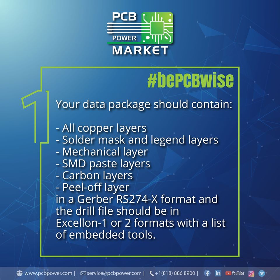
#bePCBWise - Your data package should contain:
- All copper layers
- Solder mask and legend layers
- Mechanical layer
- SMD paste layers
- Carbon layers
- Peel-off layers
in a Gerber RS274-X format and the drill file should be in Excellon-1 or 2 formats with a list of embedded tools.
#bePCBWise
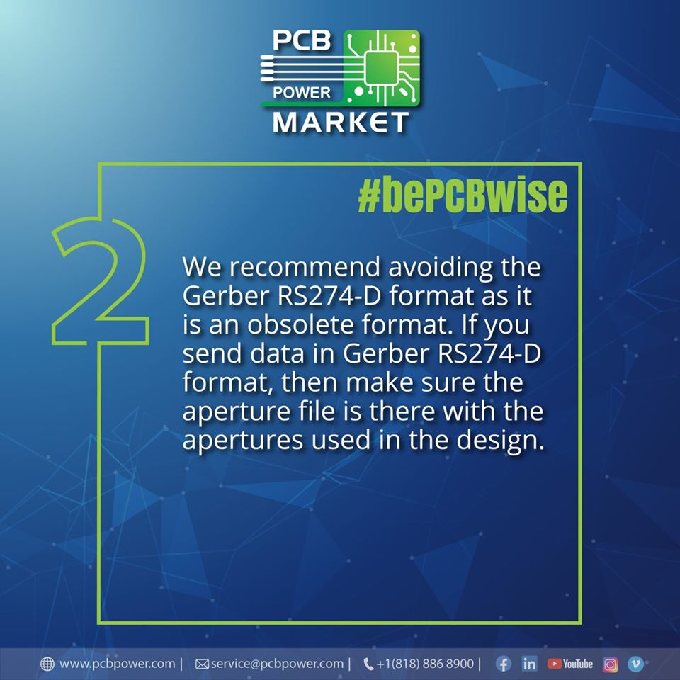
We recommend avoiding the Gerber RS274-D format as it is an obsolete format. If you send data in Gerber RS274-D format, then make sure the aperture file is there with the aperture file is there with the apertures used in the design.
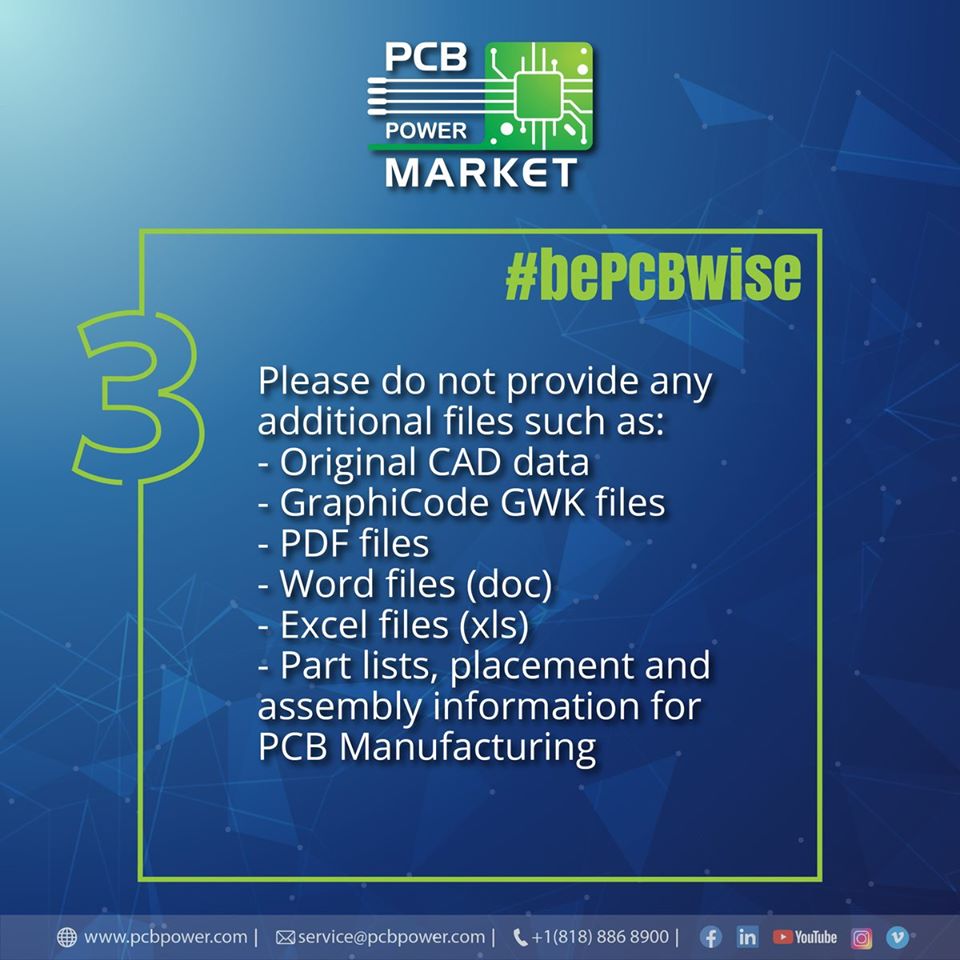
#bePCBWise - Please do not provide any additional files such as:
- Original CAD data
- GraphiCode GWK files
- PDF files
- Word files(doc)
- Excel files(xls)
- Part lists, placement and assembly infomation for PCB Manufacturing
#bePCBWise
Please check your generated output data (Gerber & Excellon) with a Gerber viewer before you send it to your PCB Manufacturer. Make sure that all the instructions or other necessary inputs needed for making the boards are included in the Gerber and Excellon files.
#bePCBWise
Please make sure that your PCB manufacturer can easily determine the layer function from the file name or add a readme file for file identification.
#bePCBWise
Please do not scale your data before you the files to your PCB manufacturer. All data provided must be scaled 1/1(100%).

#bePCBWise
Please use the same offset for all your Gerber layers and the Excellon drill data. We recommend not to use any offset.
#bePCBWise
Please use the same units (mm or inch) in your Gerber & Excellon output file as in your CAD PCB design software. This will eliminate converion or rounding errors.
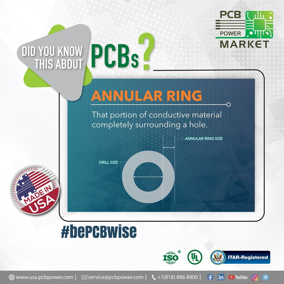
ANNULAR RING
The main purpose of an annular ring is to establish a connection between a copper pad and a trace.
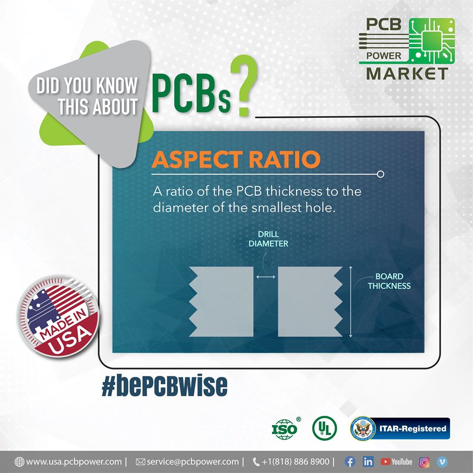
ASPECT RATIO
The aspect ratio is the thickness of a PCB divided by the diameter size of a drilled hole.
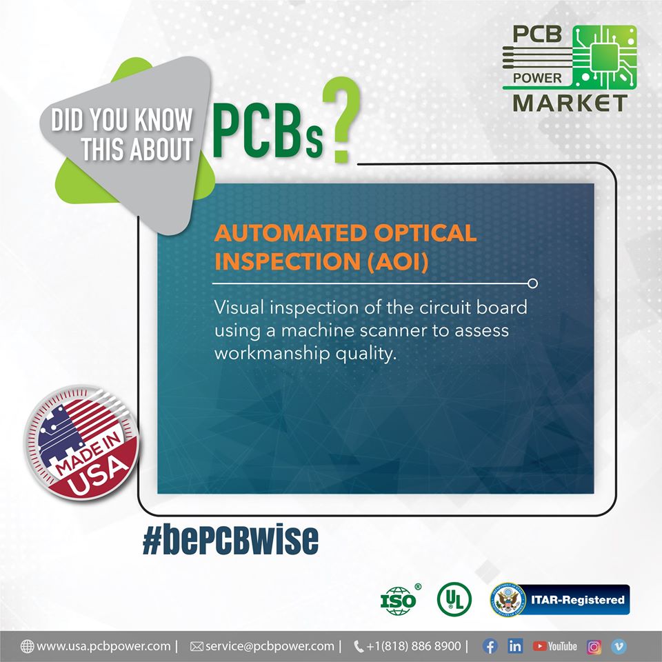
AUTOMATED OPTICAL INSPECTION (AOI)
Automated optical inspection i.e. AOI is responsible for quality control for both PCB manufacturing and PCB assembly.
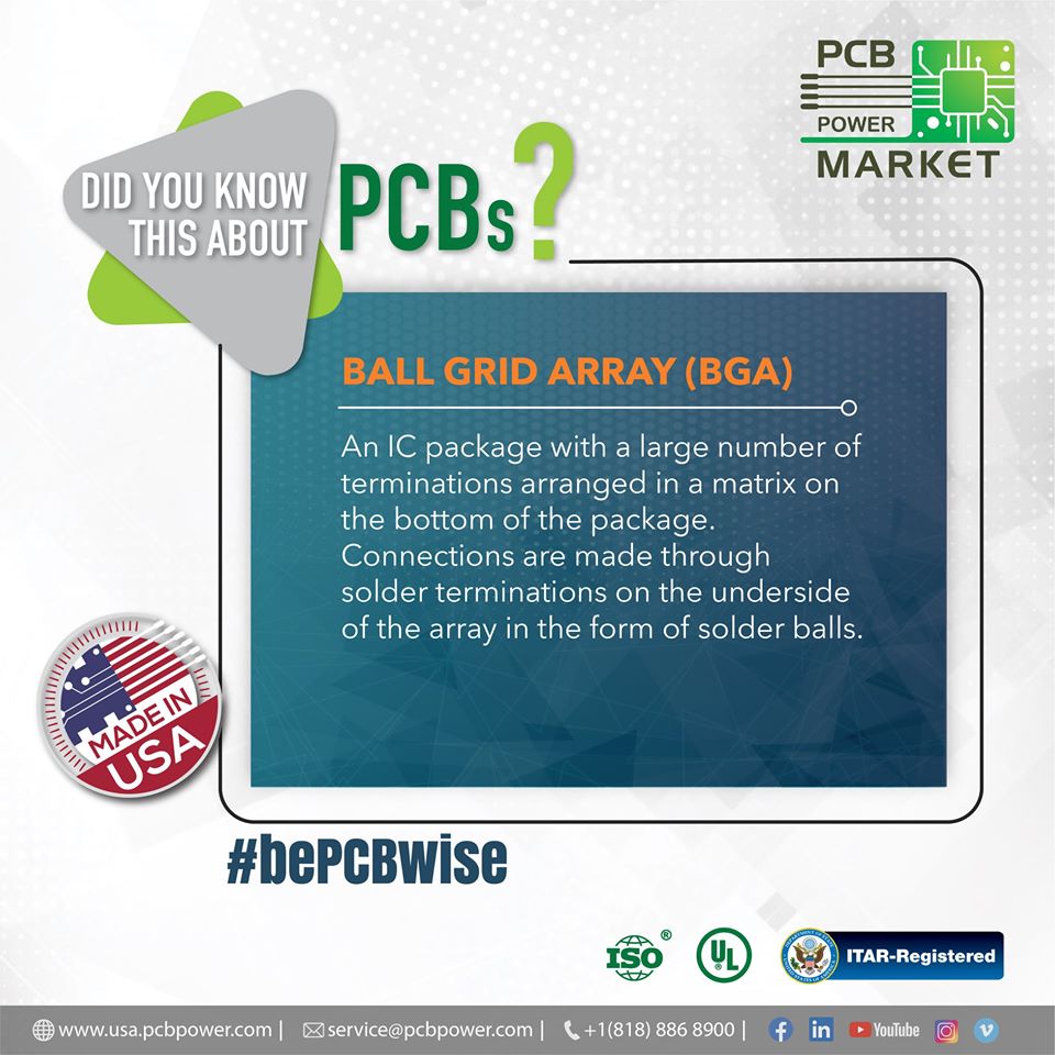
BALL GRID ARRAY (BGA)
A ball grid array (BGA) is a type of surface-mount packaging (a chip carrier) used for integrated circuits.
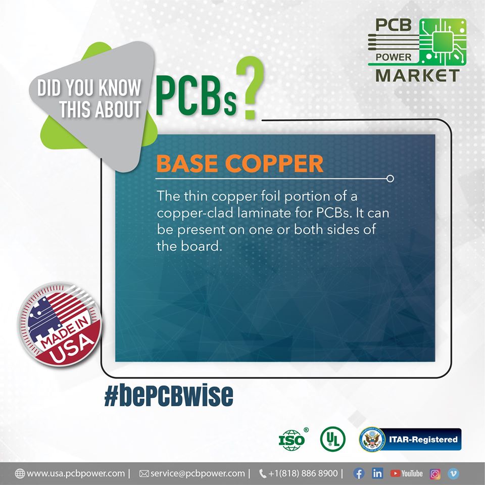
BASE COPPER
PCBs manufacturing process starts with a dielectric material with copper on both sides. This base copper is described by its weight evenly spread over one square foot.
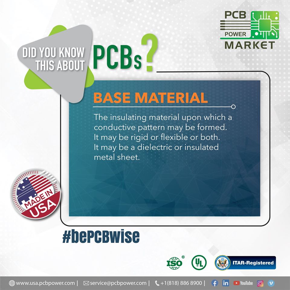
BASE MATERIAL
Base material is an important part of PCB. It determines the PCB board performance and scope of application.
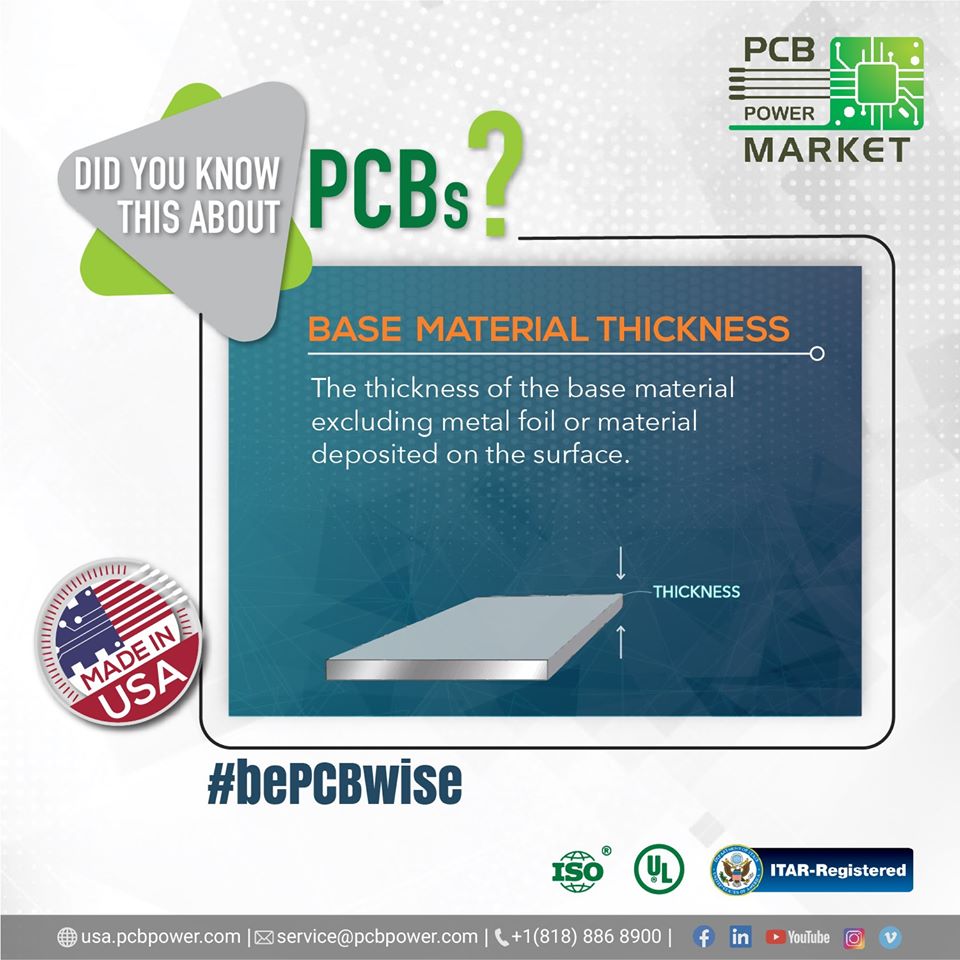
BASE MATERIAL THICKNESS
The thickness of the base metal is an important essential variable when performing weld overlays, because the thicker the base metal, the generally the weaker it is.
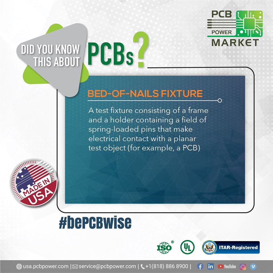
BED-OF-NAILS FIXTURE
Bed-of-Nails fixture uses a sophisticated lifting mechanism to precisely raise a platen containing the spring-loaded test probes from below the unit under test (UUT).
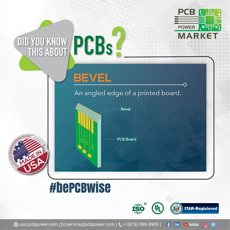
BEVEL
piece for the sake of safety, wear resistance, aesthetics or to facilitate mating with another piece.
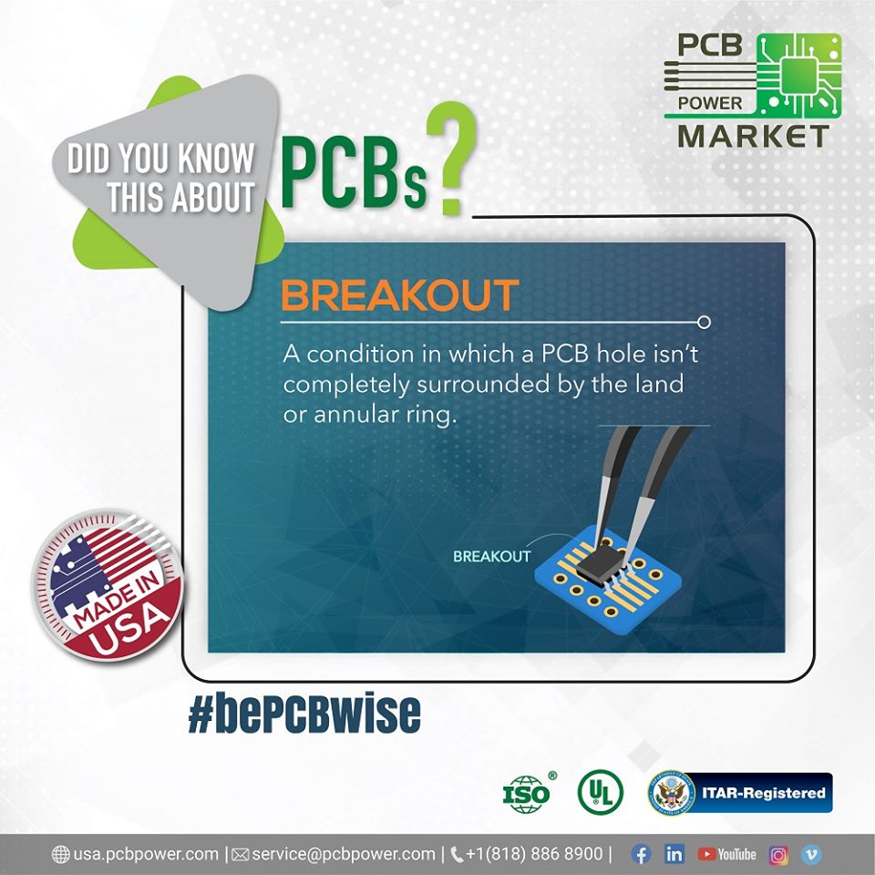
BREAKOUT
The basic concept of a breakout board that takes a single electrical component and makes it easy to use.
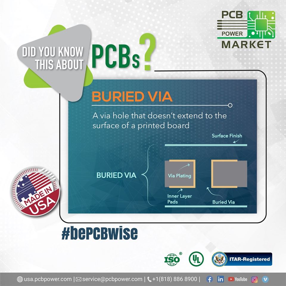
BURIED VIA
Buried Vias are used to connect between layers of a PCB where space is at a premium. It Also connects an outer layer to one or more inner layers but does not go through the entire board.
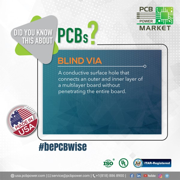
BLIND VIA
Additional Benefit of Blind Vias:
Ability to widen BGA breakout channel (layer count reduction)
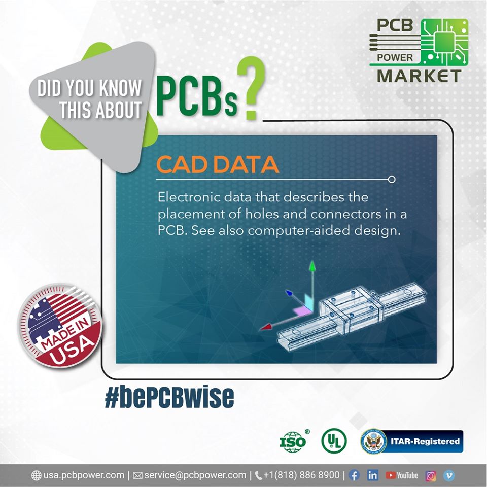
CAD DATA
CAD data exchange is a modality of data exchange used to translate data between different Computer-aided design (CAD) authoring systems or between CAD and other downstream CAx systems.
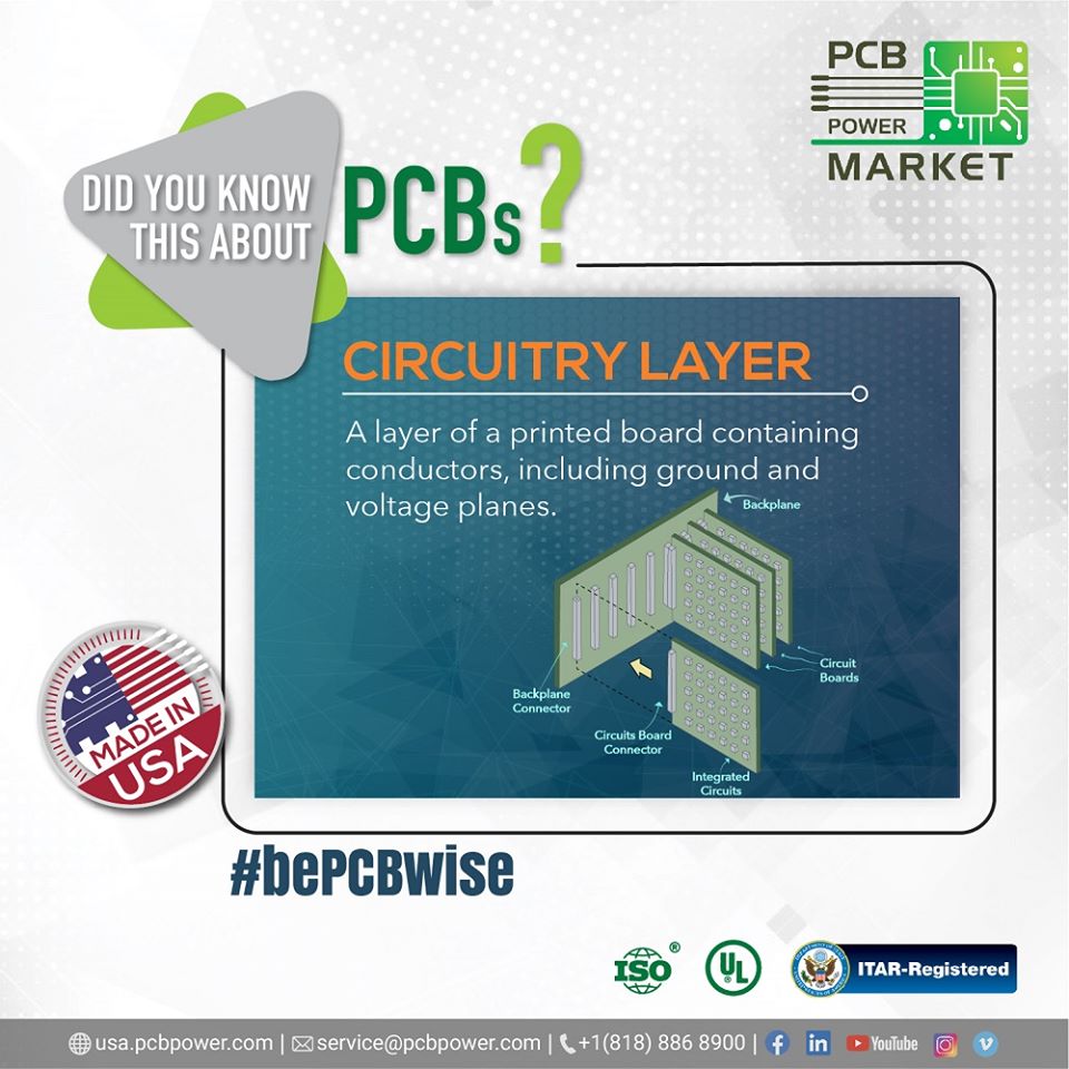
CIRCUITRY LAYER
Ground plane & voltage plane together create a large parallel plate, containing conductors is called circuitry layer.
The ground plane makes the circuit layout easier & reduces cross-talk between adjacent traces.
A power plane is responsible for distributing DC power to the active devices. It is the counterpart to the ground plane.
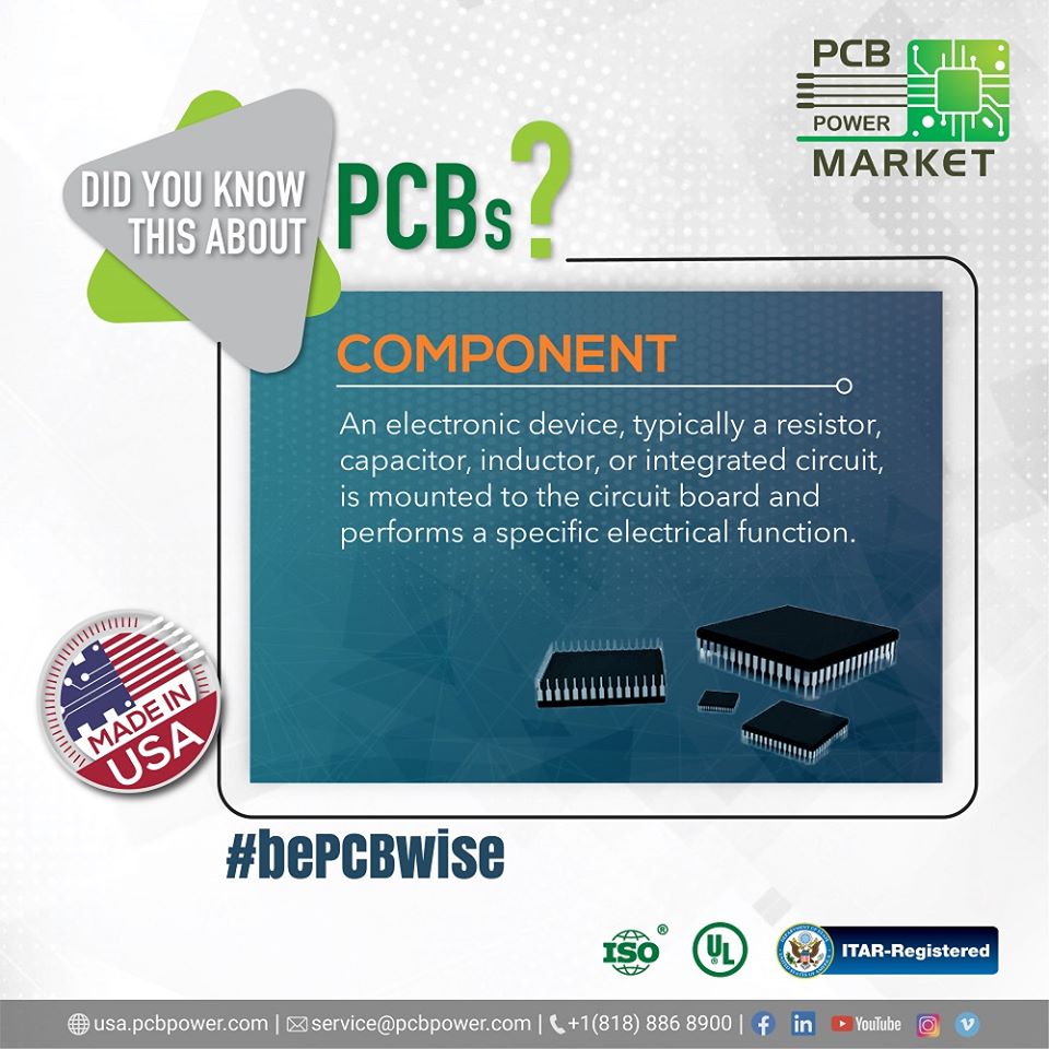
COMPONENT
If the copper plate behaves like the skeleton of the PCB, acting as its primary structure - then the components are the vital organs.
Each one has a different function. They give the circuit the unique qualities that make it fit for its intended purpose.
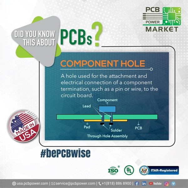
COMPONENT HOLE
Component Holes are drills for wired components used with Through-Hole Technology. In double-sided or multilayer boards the holes will be plated through.